![]()
Model 62-1 / -2
|
Table of Contents |
|
1.0 General description 2.0 Specifications 3.0 Interface Descriptions 3.1 Connector Pin-outs 3.2 User-Selectable Options 4.0 Help Appendix A Block Diagram for Model 62-1 Appendix B Block Diagram for Model 62-2 Warranty |
1.0 General descriptionThe Model 62-1/ -2 RS-232 to EIA-530 Converter is a stand-alone device
that allows conversion for the entire interface, providing ten Category-I circuits
and three Category-II circuits. The Model 62-1 includes an RS-232 port for
interfacing to a DTE, while the Model 62-2 has a port for interfacing to an RS-232
DCE. The EIA-530 port on the Model 62-1 / -2 complies with the signal characteristics of MIL-STD-188-114A, Type II. The EIA-530 specification entitled "High Speed 25 Position Interface For Data Terminal Equipment and Data Circuit Terminating Equipment" was approved March 18, 1987. The Electronic Industries Association (EIA) is changing specification nomenclature from RS-XXX to EIA-XXX. EIA-530 has been developed to serve as a complement to EIA-232-D for data rates above 20,000 bps. Together with the EIA-422-A and EIA-423-A, it provides a convenient means of implementing the higher data rates using the same mechanical connector as specified in EIA-232-D. EIA-530 is intended to gradually replace EIA-449 for the higher data rates.
|
2.0 SpecificationsSize: 5" L x 2" W x 1" H plus external power supply. Data Rate: 0 to 256 k Baud. Power: Connector is an eight-position Mini-Din female located on the side of the converter. The power cable attached to the male Mini-Din plug is connected to a low-voltage DC power supply providing +/- 12 V, +5 V and Gnd. The converters require a Telebyte Model 62-4PS independent power supply. The independent power supply requires 110 VAC and is able to provide power for one converter. See the Telebyte Model 62-4PS Reference Manual for more information. Connector: The DB-25 connector types for the Model 62-1 / -2 is described below. | ||||||||||||||||||||
|
| ||||||||||||||||||||
3.0 Interface DescriptionsThe Models 62-1 and 62-2 differ in the type of RS-232 port interfaced. The Model 62-1 is designed to interface to an RS-232 port configured as a DTE which converts the EIA-530 port to DTE. The Model 62-2 is designed to connect to an RS-232 DCE port which converts the EIA-530 port to DCE.
The phase of the signals associated with Pins 2, 3, 18, 21 and 25 are jumper selectable. There is a similarity between the RS-232 specification and the military specification MIL-STD-188C. The specifications differ in that the voltage range for the military specification is +/-6 V and the Model 62-1 / -2 drivers supply +/-10 V, although Telebyte receivers correctly decode inputs from military standard drivers. Secondly, MIL-STD-188C calls for wave shaping and the Model 62-1 / -2 has no wave shaping on the output signals. Finally, the specifications define the mark as a negative voltage whereas MIL-STD-188C define it as positive; jumpers have been provided on the data signals. To convert from RS-232 to MIL-STD-188C data signals, change jumper JP 12 and JP 14
from the factory-set positions to the inverted positions. Refer to Section 3.2.1,
"Data Signal Phasing for Model 62-1 /
-2" for more information about phasing the
data signals.
|
3.1 Connector Pin-outs
| ||||||||||||||||||||||||||||||||||||||||||||||||||||||||||||||||||||||||||||||||||||||||||||||||||||||||||||||||||||||||||||||||||||
|
Table
2: Selecting Relative Phase of Data Signals For
Model 62-1 / -2 |
|||
|
Signal |
Phasing of EIA-530 Signals |
Jumper Location |
Install Shunts |
|
TD |
Normal |
J12 |
1 to 2
3 to 4 |
|
TD |
Inverted |
J12 |
1 to 4
2 to 3 |
|
RD |
Normal |
J14 |
1 to 2
3 to 4 |
|
RD |
Inverted |
J14 |
1 to 4
2 to 3 |
|
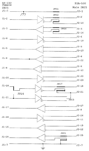
3.2.2 Data Signal Phasing for Model 62-1 The phasing of the control signals is different for the Model 62-1 than it is for the Model 62-2. The phase of the LL (J1 - Pin 18, J2 - Pin 18) and RL (J1 - Pin 21, J2 - Pin 21) signals for the Model 62-1 are affected by the shunts located at jumpers JP 16 and 17 on the main PC board and JP 23 on the upper board. The shunts allow user-selection of the phase of the signals on Pin 18 and 21 of the EIA-530 interface as well as selecting the source of those signals. There are two EIA-530 driving circuits involved with these signals. The normal configuration of the converter associates Pin 18 of each connector with each other as well as Pin 21 of each connector with each other. Refer to Appendix A, "Block Diagram for Model 62-1" or Appendix B, "Block Diagram for Model 62-2" to determine operation in other than the factory-set configurations. We do not recommended having a shunt located in JP 14 - Pin 4 and on JP 23 at the same time. This puts two drivers on J2 - Pin 21. The relative phasing of the TM signal (J1 - Pin 25 and J2 - Pin 25) is affected by
jumper position JP 21, located on the upper PC board. Refer to the
following table to determine the jumper configuration for your specific application.
| ||||||||||||||||
|
The signals with user-selectable phase and origin are LL, RL and TM. Signals LL and RL (J1 and J2, Pins 18 and 21) are affected by jumpers JP 17 on the main assembly and JP 22 on the upper PC board. Jumper JP 21 affects the signal TM and is located on the upper board. The factory settings for the LL and RL signals is for normal phasing. Refer to Appendix B, "Block Diagram for Model 62-2" for other configurations. The factory setting for the TM signal is for normal phasing. Refer to the
following table to determine the correct configuration.
| ||||||||||||||||
4.0 HelpIf you require assistance, please visit our Technical Support Center.
|
Appendix A
Block Diagram
|
|
|
Appendix B
Block Diagram
| ||||||||||
|
WarrantyTELEBYTE warrants the equipment to be free from defects in material and workmanship, under normal and proper use and in its unmodified condition, for 12 months, starting on the date it is delivered for use. TELEBYTE's sole obligation under this warranty shall be to furnish parts and labor for the repair or replacement of products found by TELEBYTE to be defective in material or workmanship during the warranty period. Warranty repairs will be performed at the point of manufacture. Equipment approved for return for warranty service shall be returned F.O.B. TELEBYTE factory and will be redelivered by TELEBYTE freight prepaid, except for non-continental U.S.A. locations. Non-continental deliveries will be sent COD freight plus import/export charges. The above warranty is in lieu of all other warranties, expressed or implied, statutory or otherwise, including any implied warranty of merchantability or fitness for a particular purpose. TELEBYTE shall not be liable for any damages sustained by reseller or any other party arising from or relating to any equipment failure, including, but not limited to consequential damages nor shall TELEBYTE have any liability for delays in replacement or repair of equipment. Out of warranty equipment may be returned to the Greenlawn, NY customer service facility prepaid as described above. Return shipping charges will be billed to the customer. The repaired unit will have a 90-day warranty. In those cases where "NO TROUBLE" is found, a reduced charge will be billed to cover handling, testing and packaging. Whether in or out of warranty, a Return Material Authorization (RMA) number is necessary and can be obtained by visiting our Technical Support Center. Reference the RMA number on the outside container. Document No. 0315-0062/Rev. D
|